Surface finish plays a crucial role in PCB production as it serves multiple purposes. Firstly, it acts as a protective layer to prevent copper oxidation, which could render the PCB non-functional. Secondly, it provides a smooth surface that facilitates the soldering of components onto the PCB.
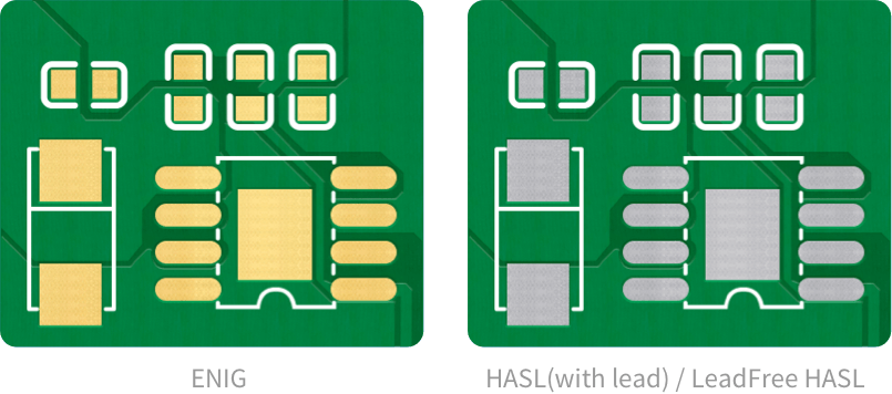
HASL (Hot Air Solder Leveling) is a cost-effective surface finishing option that involves the application of a thin protective layer of tin/lead on the PCB.
ENIG (Electroless Nickel Immersion Gold) has emerged as the industry's preferred surface finish due to its advantages, including a flat surface, lead-free and RoHS compliance, extended shelf life, and the ability to maintain tighter tolerances for plated holes.
OSP(Organic Solderability Preservatives) is also known as anti-tarnish. It involves the formation of an organic protective layer on clean and bare copper through adsorption.
ENEPIG (Electroless Nickel Electroless Palladium Immersion Gold) is a surface finish similar to ENIG (Electroless Nickel Immersion Gold) in that both processes involve the deposition of electroless nickel on top of copper plating. The key distinction is that while ENIG has gold directly deposited on top of the nickel layer, ENEPIG incorporates an additional layer of palladium between the nickel and final gold layer.